Artificial intelligence (AI), a key driver for what is expected to be a trillion-dollar industry by 2030, is placing new focus on semiconductor performance. Some of the most complex problems in delivering next-generation AI capabilities come from device fabrication challenges that will need to be addressed by new etch technologies.
Why does AI create special pressure on etch? The basic driver is the massive quantity of data needed for AI training. These in turn require high levels of parallel processing, abundant non-volatile memory (such as NAND), and fast data transfer rates to push the data into and out of memory. Advanced devices rely on architectures that are fabricated in three dimensions. As a subtractive process, etch is a powerful tool in shaping them. Gate-all-around (GAA) transistors, 3D NAND memory with low cost-per bit, and high bandwidth memory are integral to AI’s future and all need new, novel etch approaches to sculpt their device structures.
Etch has always been a critical and challenging process, but the chips powering AI will drive this to a new level. They demand not only unprecedented etch precision, but also the ability to selectively remove one material while leaving another in place, modify surface characteristics of the remaining materials, etch structures with ever-higher aspect ratios, and sometimes even etch laterally rather than only vertically.
Perpendicular Etch for AI Logic
For decades, anisotropic directional etch, selectively removing material in one direction, has been an invaluable tool for integrated circuit fabrication. Dry plasma reactive ion etch has been used to enable low-κdual-damascene interconnects, high-κmetal gates, FinFETs, buried gate DRAM, and multiple generations of 3D NAND. But the shift in recent years toward GAA transistor architectures has required a new and challenging approach: isotropic, highly selective etch. With isotropic etch, rather than etching only from the top of the stack down, uniform amounts of materials are removed in multiple directions simultaneously – a process known as perpendicular etch.

As shown in Figure 1, GAA architectures have stacks of channels, each surrounded on four sides by the gate. Perpendicular etching enables chipmakers to create these channels by using a lateral material removal process. With careful, highly controlled, angstrom-level precision, films are laterally subtracted relative to another through advanced chemistry, without loss or damage to the neighboring silicon. This process is extremely complicated and sensitive.
Another example of the need for perpendicular etching is seen with active GAA transistor surfaces. These need to be free of native oxides, residual carbon and embedded impurities. For these cases, where only a single atomic layer needs to be modified or decontaminated, a radical or neutral-based etch process provides the necessary precision while being extremely gentle.
Aspect-Ratio-Dependent Etch for Non-Volatile Memory
In addition to driving excellent cost-per-bit performance, the transition from planar (2D) to 3D NAND architecture decoupled memory capacity from feature-size scaling, which had been heavily dependent on advancements in lithography technology. Instead, storage capacity now increases with the number of device layers, largely shifting the burden onto advancements in etch and deposition processing.
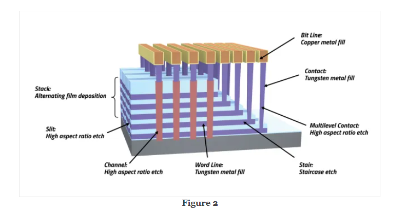
Some elements of 3D NAND structures, such as the memory channels seen in Figure 2, require etching through hundreds of layers of silicon dioxide and silicon nitride. The ratio of depth to width (aspect ratio) can be 40:1 or more — roughly the proportions of a telephone pole — and a single wafer can have over a trillion channels.
In response to this industry challenge, etch technologies have evolved to deliver highly energetic ions capable of sustaining reaction rates with good profile control, even as the structures being etched get deeper. These solutions must work together so that, for instance, etching deeper or faster does not degrade the profile of finished features. Lam Research has successfully advanced NAND channel etch using a combination of power scaling to drive ion energy; advanced wafer temperature controls (including cryogenic temperatures) to regulate reaction rates and sticking coefficients on the wafer; and novel etch chemistries for added synergies that deliver efficient, cost-effective processes.
Enabling AI Enables Etch Development
Even as etch innovations help create chips that enable the advancement of AI, conversely AI can enable the advancement of etch processes by spurring transformation in R&D and manufacturing.
AI-based predictive modeling techniques are accelerating R&D and enabling chipmakers to get to the manufacturing step faster, while giving tool and process developers new insights and greater efficiency. We are already seeing how virtual process development, using computational representations of the wafer surface and 3D simulations of device structures, can complement traditional development on physical tools with greatly increased speed and reduced cost. And the increasing number of on-tool sensors is enabling virtual metrology on fab lines for rapid identification of deviations and application of corrective actions for chamber matching and fleet optimization.
Even more exciting is a recent Lam Research study that provided process engineers with assistance from AI in a hybrid “human first, computer last” development model. It found that development costs could be cut in half while accelerating the task of pinpointing optimal etch process recipes from among millions of options. AI-aided R&D and manufacturing are still in their early days, but the potential is enormous.
Conclusion
Despite the complexity of manufacturing advanced chips, innovation in etch technology is rising to meet the demands of the AI era. Driven by extreme precision and selectivity, both perpendicular and aspect-ratio-dependent etch can address some of the most difficult manufacturing challenges.
About US
Heisener Electronic is a famous international One Stop Purchasing Service Provider of Electronic Components. Based on the concept of Customer-orientation and Innovation, a good process control system, professional management team, advanced inventory management technology, we can provide one-stop electronic component supporting services that Heisener is the preferred partner for all the enterprises and research institutions.